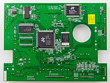
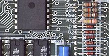
Introduction to Printed Circuit Boards
– PCBs are used to connect or wire components in a circuit.
– They consist of conductive and insulating layers.
– Electrical components are fixed to conductive pads on the outer layers.
– Vias are added to allow interconnections between layers.
– PCBs are used in nearly all electronic products.
Advantages and Alternatives
– PCBs require additional design effort but can be automated for manufacturing and assembly.
– Mass-producing circuits with PCBs is cheaper and faster than other wiring methods.
– Alternatives to PCBs include wire wrap and point-to-point construction.
– PCBs can be single-sided, double-sided, or multi-layer.
– Multi-layer PCBs allow for higher component density but make repair and modification more difficult.
History of Printed Circuit Boards
– Before PCBs, circuits were wired point-to-point on a chassis.
– Development of modern PCB methods started in the early 20th century.
– Inventors like Albert Hanson and Thomas Edison experimented with conductors on insulating boards.
– Max Schoop obtained a patent for flame-spraying metal onto a board.
– John Sargroves developed the Electronic Circuit Making Equipment (ECME) in 1936.
– Paul Eisler invented the printed circuit in the 1930s.
– Multi-layer PCBs were used in German magnetic influence naval mines during World War II.
– The USA began using PCBs on a large scale for proximity fuzes.
– The Centralab Division of Globe Union proposed a viable method for producing PCBs.
– Harry W. Rubinstein received recognition for his contributions to printed electronic circuits.
– Printed circuits became commonplace in consumer electronics in the mid-1950s.
– The Auto-Sembly process, developed by the US Army, played a significant role.
– Motorola adopted plated circuits in home radios after years of research.
– Hallicrafters released its first foto-etch printed circuit product.
– PCBs were introduced to reduce the size, weight, and cost of circuitry.
Recent advances in PCB technology
– 3D printing allows for layer-by-layer creation of PCBs.
– HDI technology enables denser designs and smaller PCBs.
– HDI PCBs use blind/buried vias and microvias for enhanced reliability.
– HDI technology is commonly used in computer, mobile phone, medical, and military equipment.
– HDI technology can reduce costs compared to through-hole PCBs.
Composition and Layers of a PCB
– A basic PCB consists of an insulating material and a layer of copper foil.
– Chemical etching divides the copper into tracks, pads, vias, and other features.
– The tracks function as wires and are insulated from each other.
– A solder resist coating protects the copper and prevents solder shorts.
– The artwork is the pattern etched into each copper layer of a PCB.
– PCBs can have multiple layers of copper arranged in pairs.
– The number of layers and interconnections indicate the board complexity.
– Two-layer boards are the simplest, while four-layer boards offer more routing options.
– Multi-layer boards have alternating layers of copper and insulation.
– Inner copper layers are protected by adjacent substrate layers.
– Through-hole components are mounted by passing wire leads through the board and soldering to traces on the other side.
– Surface mount components are attached by their leads to copper traces on the same side of the board.
– PCBs may use both through-hole and surface mount methods for mounting components.
– Through-hole mounting is less common now, with surface mounting used for most components. Source: https://en.wikipedia.org/wiki/Circuit_board
A printed circuit board (PCB), also called printed wiring board (PWB), is a medium used to connect or "wire" components to one another in a circuit. It takes the form of a laminated sandwich structure of conductive and insulating layers: each of the conductive layers is designed with an artwork pattern of traces, planes and other features (similar to wires on a flat surface) etched from one or more sheet layers of copper laminated onto and/or between sheet layers of a non-conductive substrate. Electrical components may be fixed to conductive pads on the outer layers in the shape designed to accept the component's terminals, generally by means of soldering, to both electrically connect and mechanically fasten them to it. Another manufacturing process adds vias, plated-through holes that allow interconnections between layers.


Printed circuit boards are used in nearly all electronic products. Alternatives to PCBs include wire wrap and point-to-point construction, both once popular but now rarely used. PCBs require additional design effort to lay out the circuit, but manufacturing and assembly can be automated. Electronic design automation software is available to do much of the work of layout. Mass-producing circuits with PCBs is cheaper and faster than with other wiring methods, as components are mounted and wired in one operation. Large numbers of PCBs can be fabricated at the same time, and the layout has to be done only once. PCBs can also be made manually in small quantities, with reduced benefits.
PCBs can be single-sided (one copper layer), double-sided (two copper layers on both sides of one substrate layer), or multi-layer (outer and inner layers of copper, alternating with layers of substrate). Multi-layer PCBs allow for much higher component density, because circuit traces on the inner layers would otherwise take up surface space between components. The rise in popularity of multilayer PCBs with more than two, and especially with more than four, copper planes was concurrent with the adoption of surface mount technology. However, multilayer PCBs make repair, analysis, and field modification of circuits much more difficult and usually impractical.
The world market for bare PCBs exceeded $60.2 billion in 2014 and is estimated to reach $79 billion by 2024.
