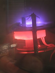
Types of Chemical Vapor Deposition
– Hot-wall thermal CVD (batch operation type)
– Plasma assisted CVD
– Atmospheric pressure CVD (APCVD)
– Low-pressure CVD (LPCVD)
– Ultrahigh vacuum CVD (UHVCVD)
– Aerosol assisted CVD (AACVD)
– Direct liquid injection CVD (DLICVD)
– Hot wall CVD
– Cold wall CVD
– Microwave plasma-assisted CVD (MPCVD)
– Plasma-enhanced CVD (PECVD)
– Remote plasma-enhanced CVD (RPECVD)
– Low-energy plasma-enhanced CVD (LEPECVD)
– Atomic-layer CVD (ALCVD)
– Combustion chemical vapor deposition (CCVD)
– Hot filament CVD (HFCVD)
– Hybrid physical-chemical vapor deposition (HPCVD)
– Metalorganic chemical vapor deposition (MOCVD)
– Rapid thermal CVD (RTCVD)
– Vapor-phase epitaxy (VPE)
Uses of Chemical Vapor Deposition
– Deposition of conformal films
– Atomic layer deposition
– Gallium arsenide for integrated circuits and photovoltaic devices
– Wear-resistant carbides and nitrides
– Polymerization for super-thin coatings with desirable qualities
Silicon Dioxide Deposition
– Silane or hydrogen-based solution used as feedstock
– Growth rate between 10 and 20 nm per minute
– Doping with phosphine, arsine, or diborane
– Silane produces lower-quality oxide than other methods
– CVD oxide has lower quality than thermal oxide
– Impurities in Silicon Dioxide
– Oxide can be grown with impurities for doping purposes
– Phosphorus pentoxide used to smooth out uneven surfaces
– Borophosphosilicate glass undergoes viscous flow at lower temperatures
– Phosphorus oxide can interact with moisture to produce phosphoric acid
– Byproducts of deposition include hydrogen and chlorine impurities
Silicon Nitride Deposition
– Silicon nitride used as insulator and chemical barrier in IC manufacturing
– Deposition from gas phase using SiH or SiCl
– LPCVD-deposited silicon nitride contains up to 8% hydrogen
– Plasma deposition of SiNH results in films with less tensile stress
– Silicon nitride has higher resistivity and dielectric strength than other insulators
Metal Deposition
– Tungsten CVD achieved from tungsten hexafluoride
– Copper deposition not commercially cost-effective using CVD
– Aluminium deposited from organoaluminium compounds
– Molybdenum, tantalum, titanium, and nickel widely used in CVD
– Metal chloride deposition and carbonyl decomposition reactions used
Graphene Synthesis
– Methane gas commonly used as carbon source for graphene
– Hydrogen required during preparation process to promote carbon deposition
– Catalysts such as iron nanoparticles and nickel foam used to change graphene production process
– Physical conditions like pressure, temperature, and carrier gas affect graphene production
– LPCVD and APCVD commonly used, with low pressures and high temperatures
Energy Costs
– Hydrogen gas and inert gases like argon are used as carrier gases in CVD.
– These gases enhance surface reactions and improve the reaction rate, leading to increased deposition of graphene.
– Standard quartz tubing and chambers are commonly used in CVD of graphene due to their high melting point and chemical inertness.
– Quartz does not interfere with any physical or chemical reactions during the process.
– Raman spectroscopy, X-ray spectroscopy, transmission electron microscopy (TEM), scanning electron microscopy (SEM), and atomic force microscopy (AFM) are used to analyze and characterize graphene samples.
Graphene Nanoribbon
– Graphene nanoribbons with widths less than 10nm exhibit electronic bandgaps, making them potential candidates for digital devices.
– Precise control over their dimensions is challenging, and rough edges negatively affect their performance.
– Graphene nanoribbons lack a bandgap between the conduction and valence bands, making them unsuitable as transistors for future digital devices.
– Despite this limitation, graphene nanoribbons have exciting electronic and thermal properties.
– The absence of a bandgap in graphene nanoribbons makes it impossible to switch between on and off states with respect to electron flow.
Diamond
– CVD can be used to produce synthetic diamond by creating the necessary conditions for carbon atoms to settle on a substrate in crystalline form.
– CVD diamond growth typically occurs under low pressure and involves feeding carbon and hydrogen gases into a chamber.
– Energy sources like hot filament, microwave power, and arc discharges are used to generate a plasma for diamond growth.
– CVD allows for the growth of diamond films over large areas with control over their properties.
– Diamond films can be used for heat sinks, cutting tools, and other applications that benefit from diamond’s hardness and low wear rate.
Chalcogenides
– Mercury cadmium telluride, an alloy of CdTe and HgTe, is commercially used for detecting infrared radiation.
– Chalcogenides can be prepared from the dimethyl derivatives of the respective elements.
– Chalcogenides, like mercury cadmium telluride, have received ongoing interest in the materials sciences.
– Chalcogenides are used for various applications due to their unique properties.
– Chalcogenides are a class of compounds that contain elements from the chalcogen group, such as sulfur, selenium, and tellurium.
Recent Advances in Chemical Vapor Deposition
– 2D Materials: CVD has been instrumental in the synthesis of various two-dimensional materials, such as graphene, transition metal dichalcogenides (TMDs), and hexagonal boron nitride (h-BN).
– Nanowires and Nanotubes: CVD is used to grow Source: https://en.wikipedia.org/wiki/Chemical_vapor_deposition
Chemical vapor deposition (CVD) is a vacuum deposition method used to produce high-quality, and high-performance, solid materials. The process is often used in the semiconductor industry to produce thin films.

In typical CVD, the wafer (substrate) is exposed to one or more volatile precursors, which react and/or decompose on the substrate surface to produce the desired deposit. Frequently, volatile by-products are also produced, which are removed by gas flow through the reaction chamber.
Microfabrication processes widely use CVD to deposit materials in various forms, including: monocrystalline, polycrystalline, amorphous, and epitaxial. These materials include: silicon (dioxide, carbide, nitride, oxynitride), carbon (fiber, nanofibers, nanotubes, diamond and graphene), fluorocarbons, filaments, tungsten, titanium nitride and various high-κ dielectrics.
The term chemical vapour deposition was coined 1960 by John M. Blocher, Jr. who intended to differentiate chemical from physical vapour deposition (PVD).
