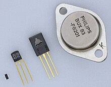
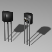
Overview and Function of Bipolar Junction Transistor
– BJT uses both electrons and electron holes as charge carriers
– Allows a small current to control a much larger current
– Uses two p-n junctions between n-type and p-type regions
– Replaced the original point-contact transistor
– Hundreds of BJTs can be made in one circuit at low cost
– BJTs exist as PNP and NPN types based on doping types of the three main terminal regions
– NPN transistor has two junctions sharing a thin p-doped region, while PNP transistor has two junctions sharing a thin n-doped region
– Charge flow in a BJT is due to diffusion of electrons and holes across junctions
– Regions of a BJT are called emitter, base, and collector
– BJTs are classified as minority-carrier devices
– BJTs can amplify input voltage or current and are characterized as current-controlled current sources
– Early transistors were made from germanium, but most modern BJTs are made from silicon
– A significant minority of BJTs are made from gallium arsenide, especially for high-speed applications
– The heterojunction bipolar transistor (HBT) can handle signals of very high frequencies
– HBT structures are usually grown by epitaxy techniques like MOCVD and MBE
Current Direction and Arrow Direction in BJTs
– Current direction on diagrams is shown as the direction a positive charge would move (conventional current)
– Current in metal conductors is generally due to the flow of electrons
– Inside a BJT, currents can be composed of both positively charged holes and negatively charged electrons
– Current arrows on diagrams show conventional direction, but labels show actual direction inside the transistor
– The arrow on the symbol for bipolar transistors indicates the p-n junction between base and emitter
– The arrow points in the direction in which conventional current travels
Voltage, Current, and Charge Control in BJTs
– Collector-emitter current can be controlled by base-emitter current or base-emitter voltage
– Current and voltage control views are related by the current-voltage relation of the base-emitter junction
– Concentration gradient of minority carriers in the base region determines collector current
– Detailed transistor models account for the distribution of charge to explain transistor behavior
– Current-control view is sometimes used in analog circuit design for its linearity
Transistor Characteristics: Alpha (α) and Beta (β)
– Alpha (α) is the proportion of carriers able to cross the base and reach the collector, indicating BJT efficiency
– Beta (β) is the common-emitter current gain, representing the ratio of collectors direct current to the bases direct current in forward-active region
– Common-emitter current gain (β) is typically greater than 50 for small-signal transistors
– Injection efficiency and recombination in the base reduce the BJT gain
– Common-base current gain (α) is the gain of current from emitter to collector in the forward-active region
– Alpha (α) and beta (β) are related by the identities: α = IC / IE, β = IC / IB, and α = β / (1 + β)
– Beta (β) is a figure of merit to describe the performance of a bipolar transistor
– Beta is assumed high enough in many designs so that base current has a negligible effect on the circuit
– Sufficient base current is supplied in switching circuits to ensure the required collector current flows
– Alpha (α) is close to unity due to the collector surrounding the emitter region, resulting in a large beta (β)
Biasing Modes and Transistor Models
– Reverse bias breakdown voltage to the base is lower in the saturation region
– In saturation mode, both junctions are forward biased, allowing high current conduction
– Cut-off mode occurs when both junctions are reverse biased, resulting in very little current
– Input characteristics and output characteristics are important in understanding transistor behavior
– The off state in digital logic involves a forward bias close to zero, resulting in no current flow
– NPN and PNP transistors have similar structures and behaviors
– In active mode, the electric field between base and collector causes electrons to cross into the collector
– The emitter current is the sum of the base and collector currents
– Increasing the base current by approximately 60mV increases the emitter current by a factor of 10
– The base, collector, and emitter currents vary in the same way
– The bipolar junction transistor (BJT) was invented by William Shockley in 1948 and was widely used for several decades
– CMOS technology has largely replaced BJTs in digital integrated circuits
– Various methods of manufacturing bipolar transistors were developed, including point-contact and junction transistors
– Large-signal models, such as the Ebers-Moll model, describe transistor currents and gains
– The Gummel-Poon model is a detailed charge-controlled model of BJT dynamics
– Small-signal models provide a more accurate representation of transistor behavior compared to the Ebers-Moll model Source: https://en.wikipedia.org/wiki/Bipolar_junction_transistor
A bipolar junction transistor (BJT) is a type of transistor that uses both electrons and electron holes as charge carriers. In contrast, a unipolar transistor, such as a field-effect transistor (FET), uses only one kind of charge carrier. A bipolar transistor allows a small current injected at one of its terminals to control a much larger current flowing between the terminals, making the device capable of amplification or switching.
 | |
| Working principle | Semiconductor |
|---|---|
| Invented | December 1947 |
| Pin configuration | Collector, base, emitter |
| Electronic symbol | |
  BJTs PNP and NPN schematic symbols | |

BJTs use two p–n junctions between two semiconductor types, n-type and p-type, which are regions in a single crystal of material. The junctions can be made in several different ways, such as changing the doping of the semiconductor material as it is grown, by depositing metal pellets to form alloy junctions, or by such methods as diffusion of n-type and p-type doping substances into the crystal. The superior predictability and performance of junction transistors quickly displaced the original point-contact transistor. Diffused transistors, along with other components, are elements of integrated circuits for analog and digital functions. Hundreds of bipolar junction transistors can be made in one circuit at very low cost.
Bipolar transistor integrated circuits were the main active devices of a generation of mainframe and minicomputers, but most computer systems now use Complementary metal–oxide–semiconductor (CMOS) integrated circuits relying on the field-effect transistor (FET). Bipolar transistors are still used for amplification of signals, switching, and in mixed-signal integrated circuits using BiCMOS. Specialized types are used for high voltage switches, for radio-frequency (RF) amplifiers, or for switching high currents.
